

Wishbone-NPU: A Neural Processing Unit for RISC-V Soft-Cores, Built by Students
A Penn State Behrend capstone team composed of Dylan Thomas Stock, Dipen Arun Rathod, and Jacob Loucks built an open-source neural processing unit in VHDL and Ada, then used it to run a 14-stage convolutional neural network (CNN) on a RISC-V soft-core processor.
Image analysis using a neural network is a common approach for training a computer to recognize specific features in images. Useful for analyzing, say, X-Ray images, or images of breast cancer to detect benign or malignant tissue. Running a neural network inference on a CPU consumes many cycles performing matrix operations. A dedicated FPGA would be a more logical choice for handling dense layers, convolutions, activations, and pooling. This makes an FPGA with a soft-core a great solution. Run a soft-core on the FPGA for the control logic, and run the neural network on the FPGA via a Wishbone connection.
That became a Penn State Behrend capstone project. Through the GNAT Academic Program, AdaCore sponsored the work, with Naseem Ibrahim advising the team and AdaCore's Olivier Henley acting as project mentor. The result is the Wishbone-NPU, an open-source hardware accelerator written in VHDL and driven by Ada firmware.
The design objective was straightforward. The NPU had to be a self-contained Wishbone B4 slave, with no dependency on a particular CPU or FPGA family. If a SoC has a Wishbone master, the NPU can be added at a base address and immediately receive tensors. The reference system combines it with a NEORV32 RISC-V soft-core on a Lattice ECP5, clocked at 72 MHz. Alire builds the complete Ada firmware stack.
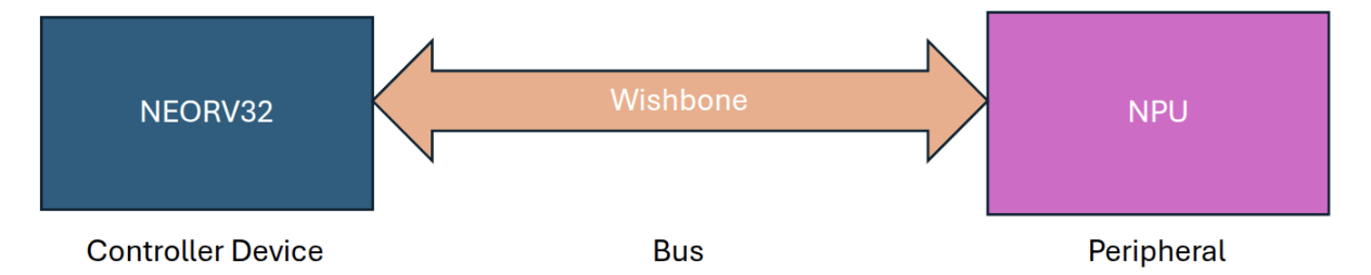
As with any software-hardware project on an FPGA, an important design decision is where the team places the boundary between hardware and software. They made that boundary explicit and applied it consistently throughout the project.
One state machine, four BRAM windows, packed INT8
Communication from the NEORV32 to the NPU happens through a flat register map and four tensor windows, all of which are memory-mapped behind the Wishbone slave port. The tensor unit in the NPU takes an input, applies the model, and generates a result. The model is represented through weights and biases, which need to be computed offline and are part of the application:

So the interface is:
- Control Register
- Tensor A: inputs, 2500 words
- Tensor B: weights, 9000 words
- Tensor C: biases, 2000 words
- Tensor R: results, 2500 words
Each word contains four INT8 values in Q0.7 format (1 sign bit and 7 fractional bits). A 100x100 grayscale image occupies exactly 2500 words, which explains the size of A and R. All seven operations, dense, conv2d, ReLU, sigmoid, softmax, max pooling, and average pooling, use a single unified FSM. A 5-bit opcode in the control register selects which of these operations to perform.
The driver protocol follows the usual peripheral handshake: write the operands, write the parameters, select the opcode, assert start, poll the busy bit, then read R.
Two low-level design decisions are particularly important.
The first is BRAM inference. Each tensor memory is read and written from a single clocked process. Its port is multiplexed between the Wishbone side when the NPU is idle and the FSM side when it is busy. This is what synthesis tools need to map arrays to block RAM rather than implement them as registers.
The second is arbitration by construction. Access to the tensor windows is acknowledged only while the NPU is idle. The CPU can always poll the control and status registers, but it cannot race the FSM on the tensor ports. There are no locks and no flags that software can forget. The bus protocol enforces mutual exclusion.
The multiply-accumulate datapath: gemmlowp in three states
The compute core uses a 4-lane MAC datapath. On each cycle, the FSM unpacks four INT8 inputs and four INT8 weights from one word each, adjusts the weights by the zero-point, multiplies each lane, and accumulates the result in a 32-bit register. A lane-count signal handles the remaining elements when a row length is not divisible by four.
Converting the 32-bit accumulator back to an INT8 activation requires requantization. The team implemented it following Google's gemmlowp guide. The Python conversion script first combines the layer scales into one real multiplier. It then encodes that value as an int32 quantized multiplier in Q0.31, together with a right-shift count.
On the FPGA, the FSM performs the conversion in three dedicated states. It multiplies the biased accumulator by the quantized multiplier to produce a 64-bit value, applies a rounded shift with the correct handling of negative values, then clamps the result to [-128, 127]. Product, shift, clamp. Each operation has its own named state and pure VHDL function.
The intermediate values are also exposed through debug registers, allowing the Ada firmware to inspect the pipeline one word at a time. That visibility becomes extremely useful when the numeric pipeline differs from Keras by one LSB.
Softmax: the division stays in Ada
Softmax requires taking exponentials, followed by division by their sum. The exponentials are handled in hardware using the linear approximation e^x is approximately 1 + x over the Q0.7 range. The approximation is applied lane-by-lane over the packed words in a single pass.
The division is handled differently. A combinational divider would consume a significant number of LUTs and make timing closure more difficult. The team therefore split softmax into two hardware passes, with Ada handling the division between them.
During the first pass, the NPU computes the exponentials in place. The Ada firmware reads them back, masks the unused lanes in the final partial word so that padding does not affect the probabilities, sums the valid elements, and computes a fixed-point reciprocal: 2^16 divided by the sum. During the second pass, the firmware writes this inverse sum to a parameter register, and the NPU multiplies every exponential by it. Multiplication maps directly to the ECP5 DSP blocks. The division is executed once in software, at a reasonable cost.
The RTL comments also explain why the sum is not accumulated in hardware. A sum register shared by both the FSM and the bus would introduce a multiple-driver problem and make the FSM larger for little benefit. The team made a clear decision about what belongs in the accelerator and what does not.
Chaining layers without a bus round-trip
A real network contains a sequence of layers. A naive driver would read every intermediate result over the bus, then write it back as the input to the next layer. The team added an opcode to avoid this: OP_COPY_R_TO_A moves N words from the result window to the input window inside the FPGA.
On the Ada side, Copy_Result_To_Input is called; the fabric performs the copy, and the intermediate tensor never crosses the bus. This is particularly important for the 14-layer camera demo.
The Ada side: a register map you can read
The firmware library, wb_npu_helper, follows a common Ada design pattern for hardware drivers.
One package, wb_npu_address_map, contains every register and tensor-window address as a typed System.Address constant. The corresponding semantics appear in a comment on the same line. The root package contains the opcodes, bit masks, and low-level operations: register setters, Perform_Op, busy polling, and word-level access to the four tensor windows. Hierarchical child packages then expose one procedure for each layer type, with an explicit signature:
procedure Apply_Dense_All_Words
  (Inputs                           : Natural;
   Neurons                          : Natural;
   Weight_Base_Index                : Natural;
   Bias_Base_Index                  : Natural;
   Zero_Point                       : Integer;
   Quantized_Multiplier             : Integer;
   Quantized_Multiplier_Right_Shift : Natural);
The procedure exposes only what the hardware requires, nothing more, and uses no hidden global state. Wb_Npu_Helper.Dense, .Conv2D, .Activation, .Pooling, and .Debug form a package tree that mirrors the hardware capabilities. A demo application, therefore, reads like the network it implements.
The model weights are generated as Ada constants. The model is trained in Keras, then processed by a conversion script that emits a package containing constant arrays: INT8 weights packed four per 32-bit word, biases stored as 32-bit words, and the zero-point, quantized multiplier, and shift for each layer.
The complete model is compiled into the executable. There is no RTOS, no filesystem, loader, or runtime parsing. Alire builds the application for riscv64-elf using a bare runtime. objcopy and the NEORV32 image_gen tool produce the executable, which is then uploaded through the UART bootloader.
The demos and the timings are the proof
There are several demonstrations in the repository. The MNIST 14x14 firmware runs a 196-to-32-to-10 MLP with ReLU and softmax on embedded test samples of handwritten digits. It records per-stage cycle counts relative to the 72 MHz clock, then reports accuracy along with the best and worst sample latencies over the UART. The project also includes 28x28 MNIST (a database of images representing handwritten digits) and variants of a breast cancer classifier based on the same architecture.
The final integration test adds a Waveshare OV5640 camera as a second Wishbone slave, connected through a small 1-master-2-slave interconnect also written by the team. The firmware captures a 100x100 grayscale frame and sends it through a 14-stage CNN. The network includes pooling, three convolution stages with ReLU, additional pooling, and two dense layers. It runs entirely on the NPU and classifies rock, paper, or scissors in real time.
The team also wrote npu_layer_worst_case_timings, a firmware test suite that fills the tensor windows with worst-case data and reports the cycle and microsecond cost of each layer as CSV over the serial port. These are measured worst-case timings for each operation on the actual hardware. This level of timing information is absent from many published accelerator projects.
Six repositories, one system
The work is distributed across six repositories that combine into one system: the NPU, the Ada IO helper library, the OV5640 camera controller, the Wishbone interconnect, a central tutorial hub, and the GNAT Academic Program's NEORV32 setup and HAL repositories that support the firmware.
Three YouTube tutorial series also explain how to run Ada on the NEORV32, connect the NPU in VHDL, and deploy trained models from beginning to end.
Limitations and Tradeoffs
The README clearly states the project's limitations. BRAM capacity limits the model size. A DMA to external HyperRAM or INT4 Q0.3 packing could address this. The single FSM processes four lanes per cycle. It could be pipelined, or the compute units could be replicated.
These are concrete engineering trade-offs, with the reasoning documented. More importantly, the students had to work across the complete system. They trained a model in Keras, quantized it using production-grade arithmetic, generated typed Ada from it, and used that code to drive custom VHDL through a memory-mapped driver library they designed themselves. They then measured worst-case behavior on real silicon.
At every step, they had to define and defend an abstraction boundary: hardware versus software, generated versus handwritten code, and register map versus driver API. This is exactly the objective of the GNAT Academic Program. Students work with real tools, real constraints, and real engineering trade-offs.
Get involved
The Wishbone-NPU is open source and available under the MIT or Apache-2.0 license. The project also provides several accessible contribution paths. Porting the peripheral to another board or implementing one of the documented improvements would make a useful first FPGA or Ada contribution. The register interface is stable, and the project leaves room for extensions.
Explore the project on GitHub, and learn more about the GNAT Academic Program.
Congratulations to the Penn State Behrend capstone team, and thanks to Naseem Ibrahim for advising the project.
FAQs
AdaCore sponsors a limited number of capstone projects at various universities per year. Feel free to reach out to your capstone director and point them to this article, and have them reach out.
For capstone projects, we typically use readily available, affordable hardware. You should be able to find these boards at your usual retailers.
Capstones rely on the open source Ada toolchain and the Alire package manager. You can download from here. The work of the academic projects is typically provided in open-source projects; links are provided in the text above
Author
Olivier Henley

The author, Olivier Henley, is a UX Engineer at AdaCore. His role is exploring new markets through technical stories. Prior to joining AdaCore, Olivier was a consultant software engineer for Autodesk. Prior to that, Olivier worked on AAA game titles such as For Honor and Rainbow Six Siege in addition to many R&D gaming endeavors at Ubisoft Montreal. Olivier graduated from the Electrical Engineering program at Polytechnique Montreal. He is a co-author of patent US8884949B1, describing the invention of a novel temporal filter implicating NI technology. An Ada advocate, Olivier actively curates GitHub’s Awesome-Ada list